Electronics Design & Build
Analog Filter Design
One input, three frequency-selective outputs: low-pass, high-pass and band-pass.
Experience In Practice
Skills Applied
Technical Skills
Soft Skills
Separate A Signal By Frequency
A single input feeds three filter responses. The low-pass output retains the slower variations below the cutoff, the high-pass output retains frequencies above it, and the band-pass output selects the region around the centre frequency.
I designed and built the circuit around a nominal 1.2 kHz centre/cutoff frequency. Taking all three outputs from the same input makes their behaviour directly comparable and illustrates how analog signal conditioning can separate useful content from unwanted frequencies.
Shape The Response Without Loading The Signal
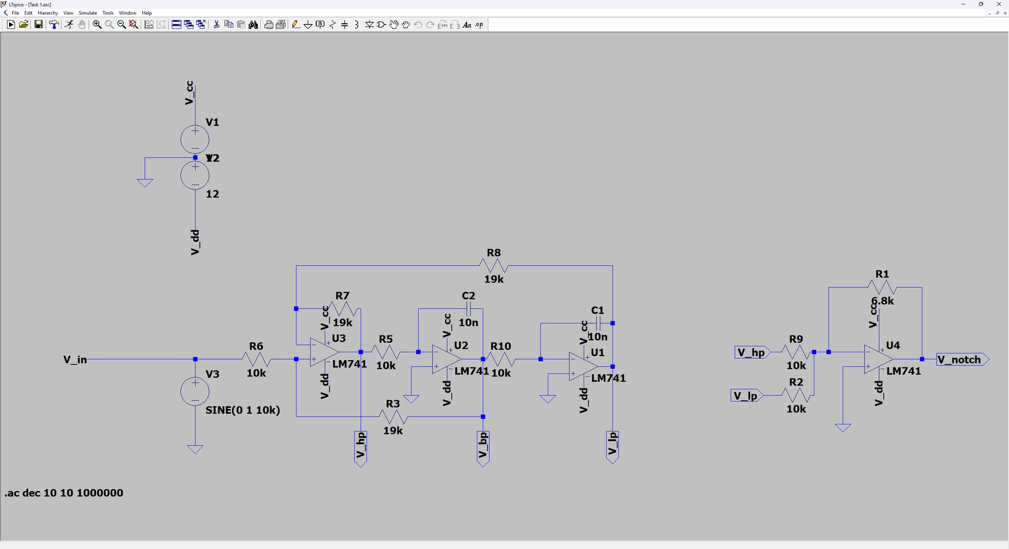
The design operates from ±12 V supplies with an input up to 1 V peak-to-peak. Its active stages combine op-amp gain and buffering with frequency-dependent resistor/capacitor networks.
The design targets were a pass-band response within ±1.5 dB of unity, at least 35 dB attenuation for the low-pass and high-pass outputs one decade from cutoff, and at least 17 dB for the band-pass output. Input impedance of at least 10 kΩ and output impedance no greater than 1 kΩ help limit loading between the source, filter and following circuit.
Component tolerances matter because resistor and capacitor variation moves the response. The circuit and component choices therefore balance the desired filtering, a compact implementation and sensitivity to manufacturing variation.
Build The Circuit And Plan The Board
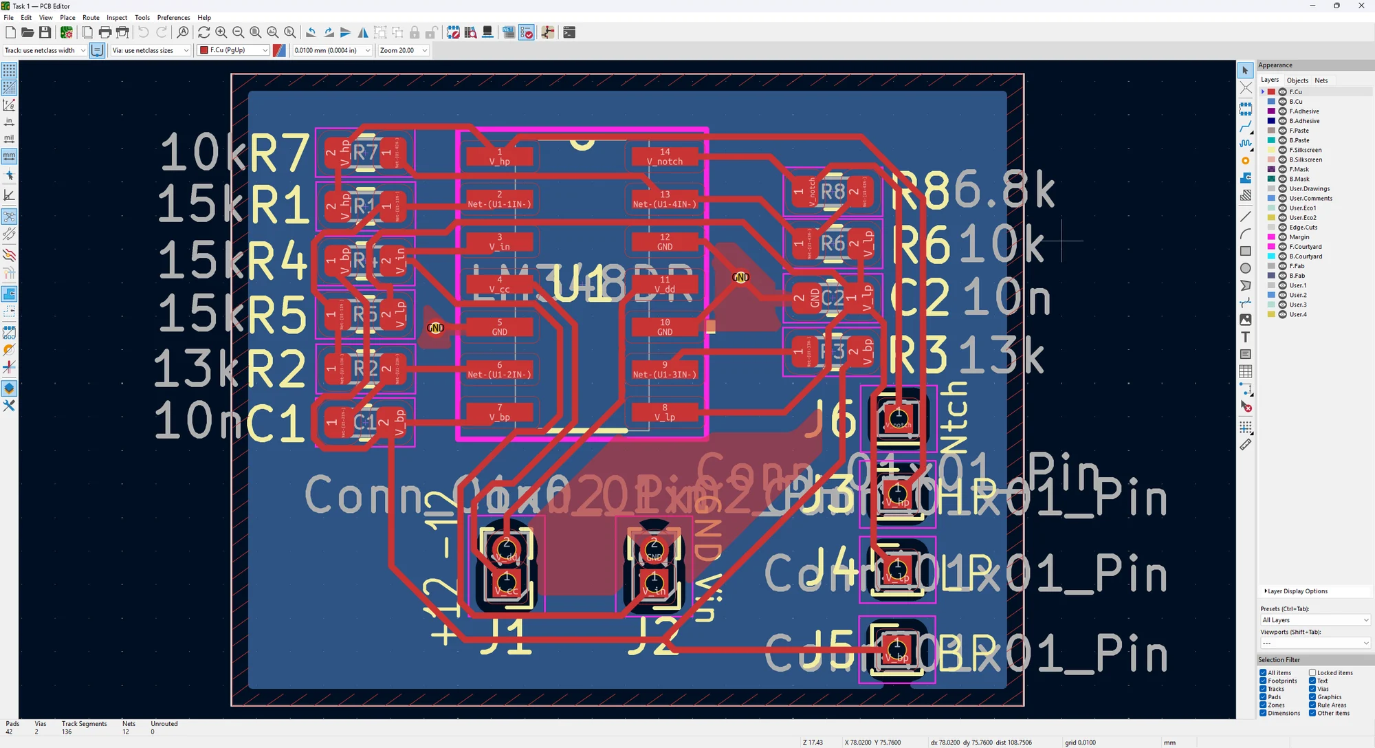
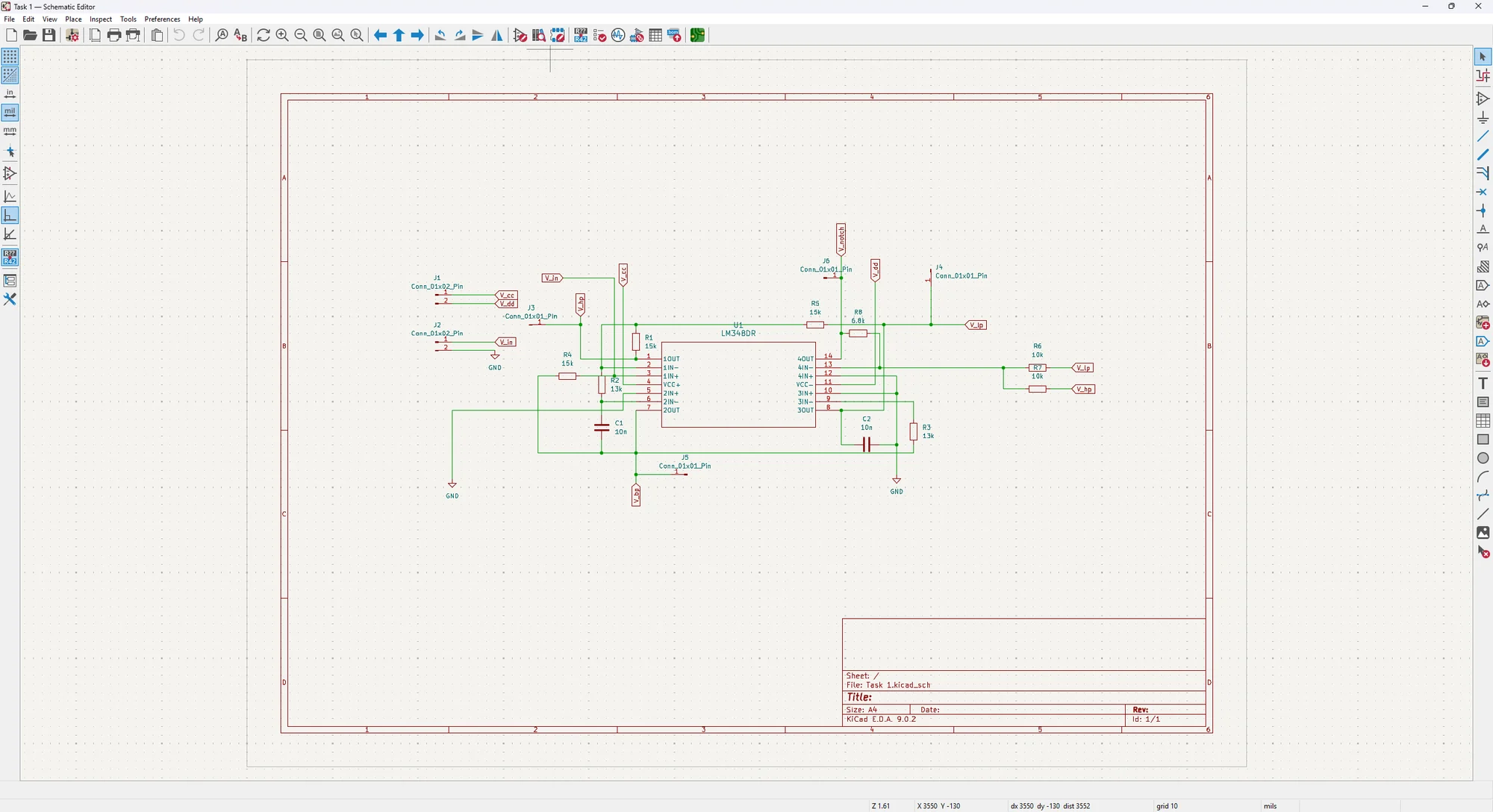
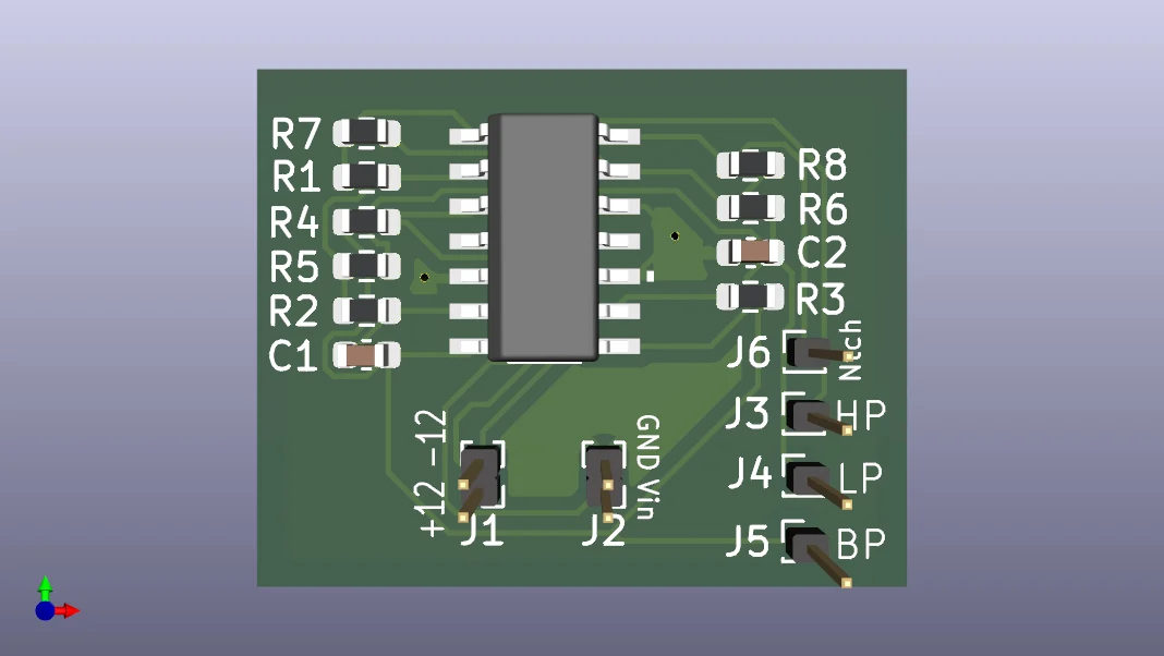
I completed the physical circuit and developed its schematic, LTspice representation, PCB routing and 3D layout. The LM348-based component list records the resistor and capacitor values, SMD footprints and quantities needed to carry the design into a board.
The gallery and bill of materials connect the electrical function to the practical implementation: how the signal is filtered, how the parts connect and which components are needed for assembly.
The Engineering Journey
Shape
Define low-pass, high-pass and band-pass responses around 1.2 kHz.
Build
Translate the active-filter circuit into a physical implementation.
Package
Develop the schematic, PCB layout and bill of materials.
What This Experience Achieved
The result
A physically built three-output analog filter, supported by circuit simulation, a PCB design and a component-level bill of materials.
From Circuit Design To Parts Selection
Bill Of Materials
The component list turns the circuit and PCB design into specified parts, footprints and quantities for sourcing and assembly. It documents the parts needed to build the design.
| Part / Value | PCB Footprint | Quantity |
|---|---|---|
| LM348 | | 1 |
| 15k | Resistor_SMD:R_0603_1608Metric | 3 |
| 13k | Resistor_SMD:R_0603_1608Metric | 2 |
| 10k | Resistor_SMD:R_0603_1608Metric | 2 |
| 6.8k | Resistor_SMD:R_0603_1608Metric | 1 |
| 10n | Capacitor_SMD:C_0603_1608Metric | 2 |
Board Requirements
- Board area
- 444.388
- No of layers
- 2
- No of vias
- 2
- Avg track length
- 12
- Longest track length
- 23.86
Values are transcribed from the design workbook. Dimensional units are not specified in the source.
Download BOM (Excel) ↓A Closer Look
Technical decisions & tools
The stated ripple, attenuation and impedance figures are design specifications. They are not a published set of measured response results.
The bill of materials specifies an LM348, 0603 resistors and capacitors. The PCB design links those footprints to the circuit connections.