Electronics Design & Build
Digital Pulse Divider
Select divide-by-one through divide-by-four operation while preserving the input pulse on-time.
Experience In Practice
Skills Applied
Technical Skills
Soft Skills
Select The Output Pulse Rate
Two digital control inputs, B1 and B0, select a binary value N from 0 to 3. The circuit produces one output pulse for every N + 1 input cycles: fout = fin / (N + 1).
The four settings are 00 → divide by 1, 01 → divide by 2, 10 → divide by 3 and 11 → divide by 4. The circuit is designed for 0–5 V TTL signals, a single 5 V supply and nominal input clocks from 1 kHz to 50 kHz.
Preserve Pulse Width As The Rate Changes
The output keeps the input pulse’s on-time while increasing the interval between output pulses. Its duty cycle therefore decreases as the division ratio increases; it is not simply a slower copy with an unchanged duty cycle.
Counting, state transitions and output gating have to agree so that transitions do not create unwanted short pulses. The timing relationship between the input clock, stored state and decoded output is central to the design.
Simplify The Logic Across Three Iterations
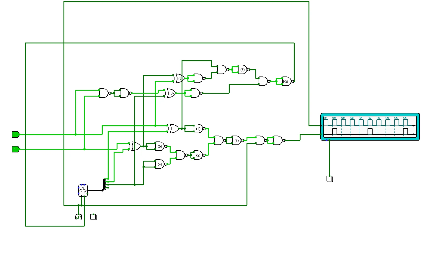
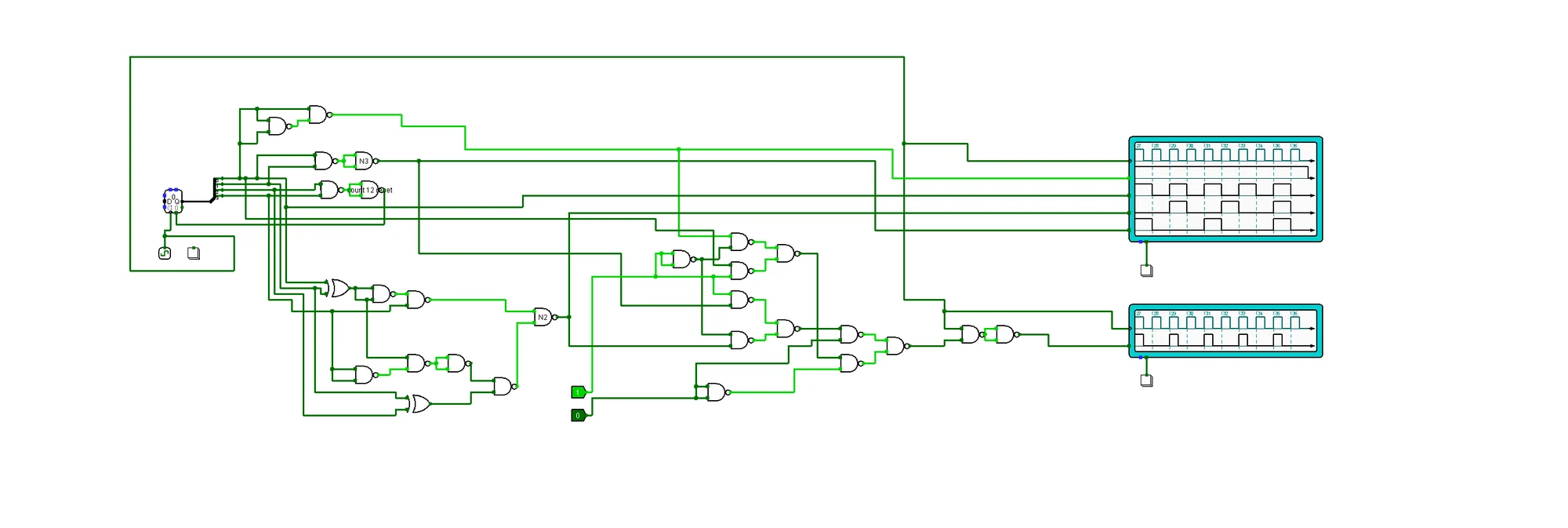
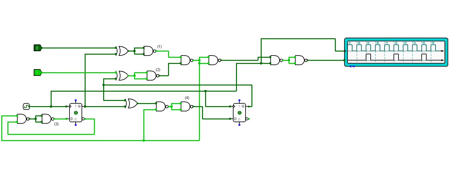
I refined the truth tables and redesigned the circuit through three solutions, progressively reducing the number of components and logic functions needed. The physical implementation is Solution 3, which I built in full.
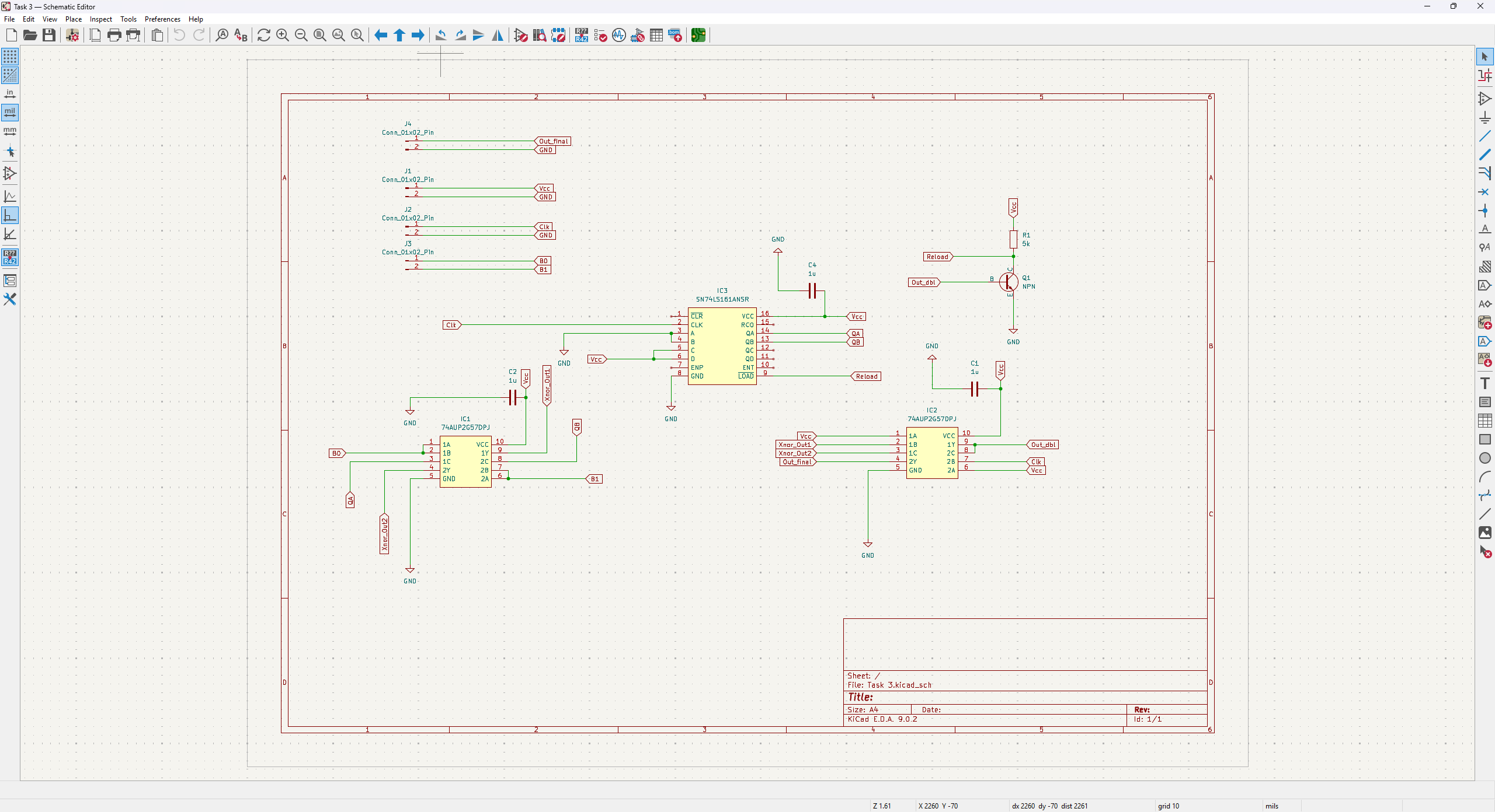
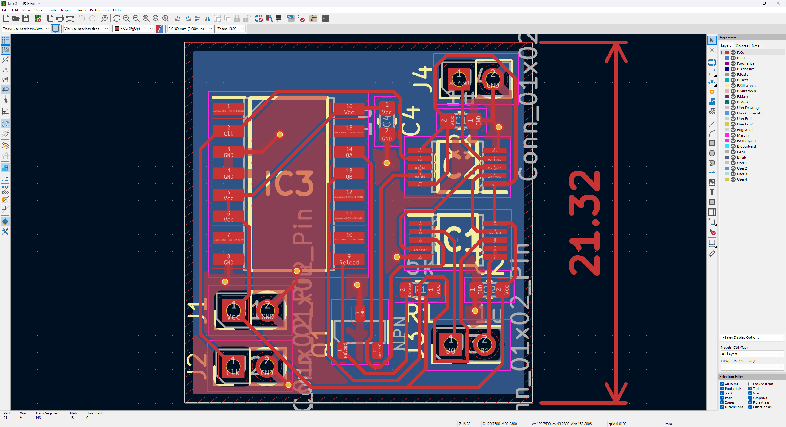
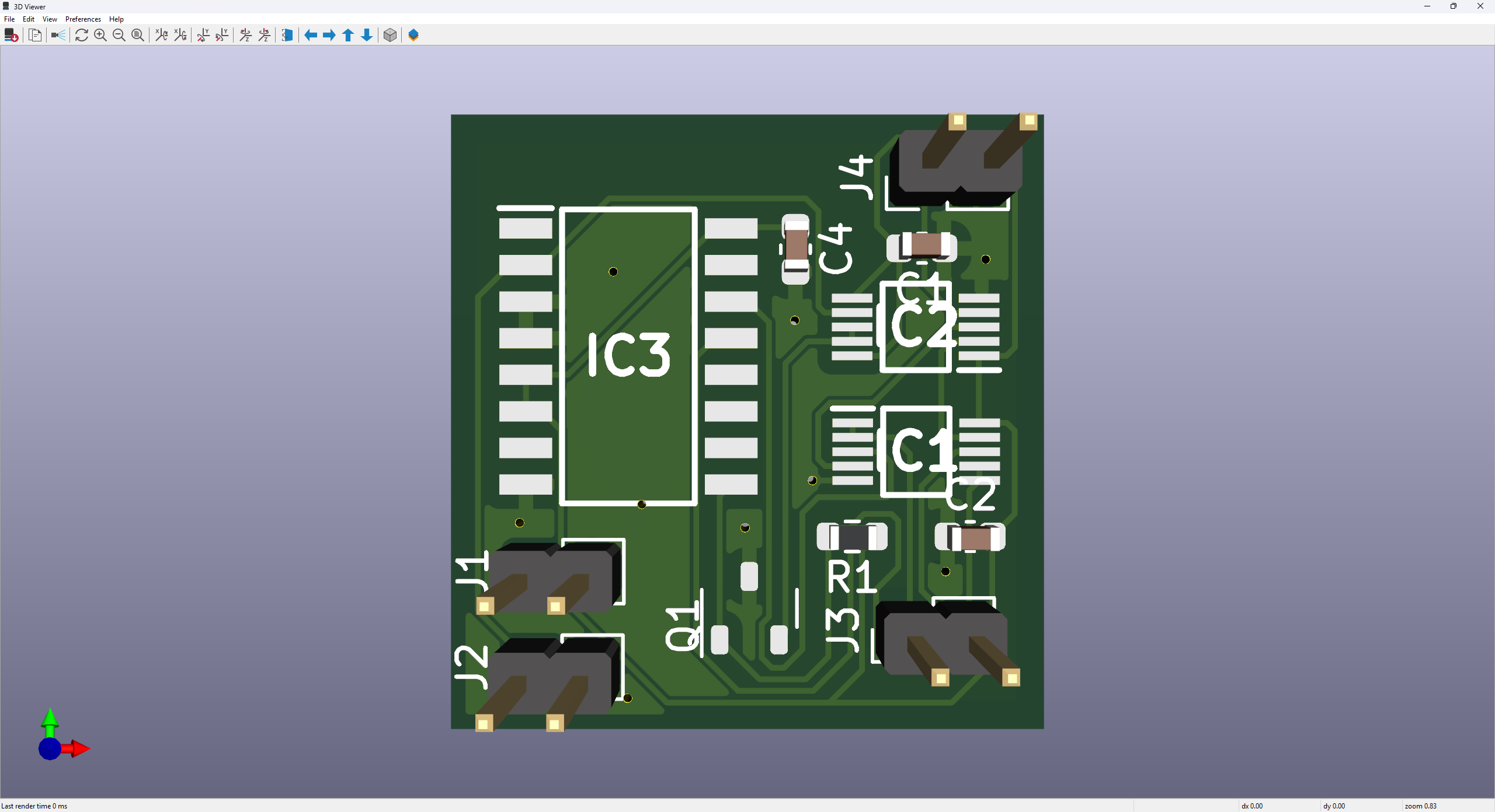
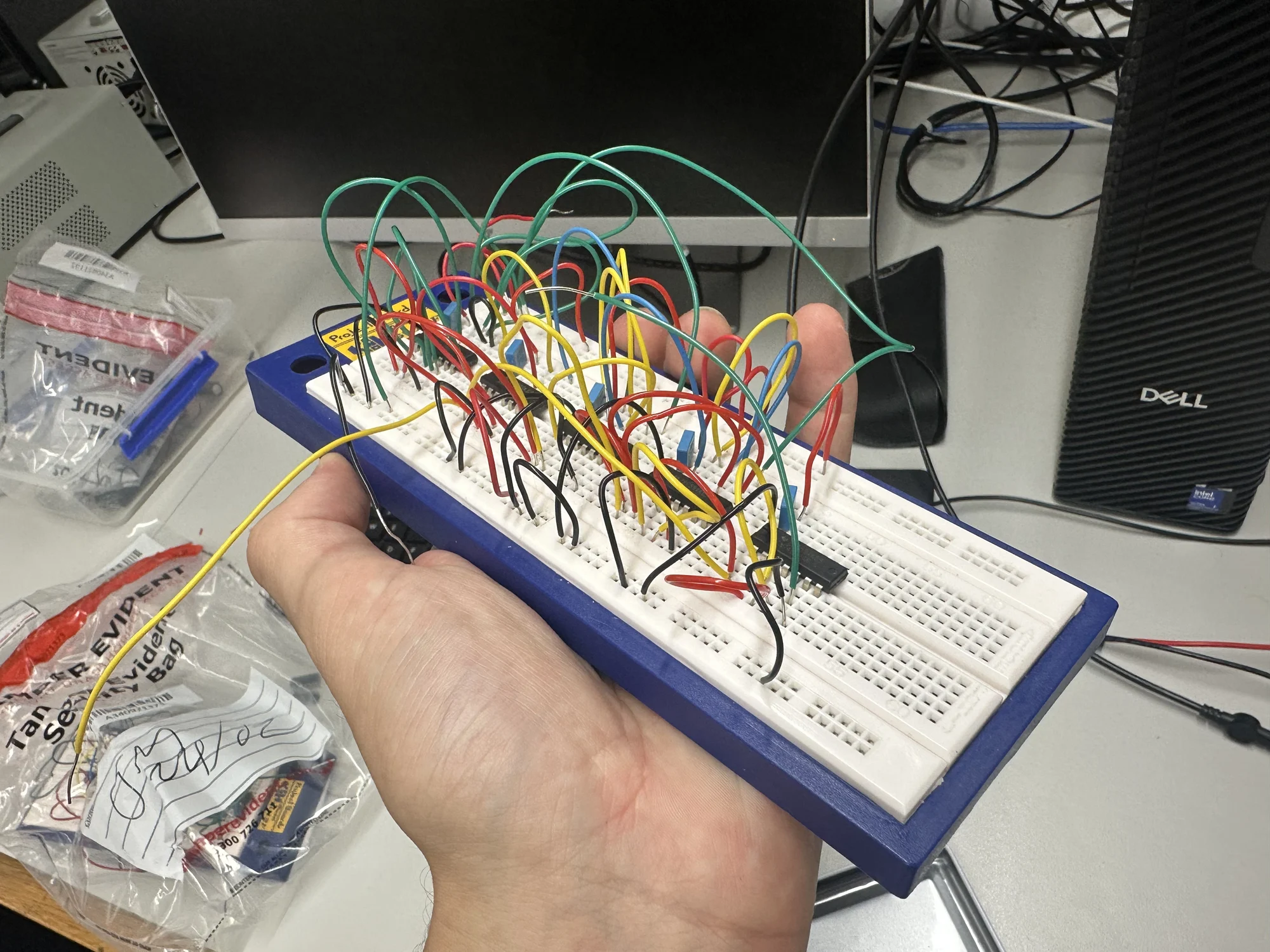
The gallery begins with the PCB schematic, layout and 3D model, then shows the built prototype and Solutions 1, 2 and 3. Together they show both the final implementation and the decisions that made it simpler.
Carry The Logic Into A Board
The PCB design translates the logic into component connections, placement and routing. Moving from logic equations to a physical layout adds practical concerns such as readable signal paths, supply connections and access to the control and output nodes.
The Engineering Journey
Analyse
Work through the truth table and first circuit.
Optimise
Redesign the logic across three iterations to reduce component count.
Build
Physically implement the third solution.
What This Experience Achieved
The result
Solution 3 physically implemented after three logic-design iterations, with a PCB schematic, routed layout and 3D model.
Technical decisions & tools
Division is by N + 1, not N: the zero control setting passes the input pulse rate through.
The specified 1–50 kHz input range and glitch-free operation are design requirements. The implementation retains the original pulse on-time as the division setting changes.